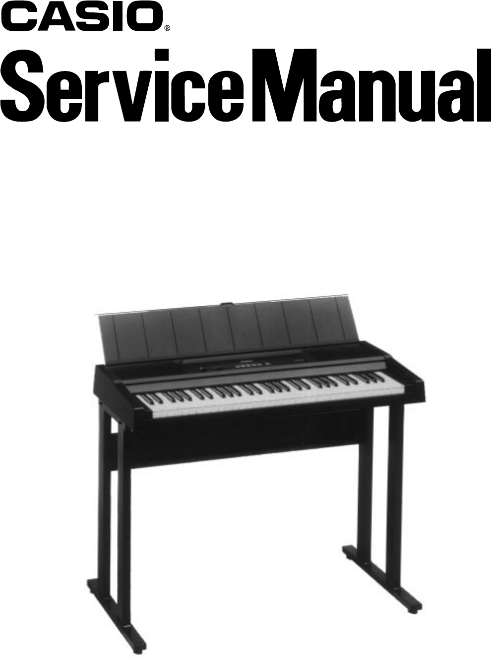
Casio CPS-130 User Manual
Browse online or download User Manual for Digital pianos Casio CPS-130. S/M CPS-130
- Page / 16
- Table of contents
- TROUBLESHOOTING
- BOOKMARKS
- ELECTRIONIC KEYBOARD 1
- SPECIFICATIONS 2
- CONTENTS 2
- BLOCK DIAGRAM 3
- KEY AND SWITCH MATRIX 4
- SCHEMATIC DIAGRAMS 5
- PCB M5312-CN1M 6
- PCBs M615K-KY1M, KY2M 7
- PCB VIEW 8
- TROUBLESHOOTING 10
- EXPLODED VIEW 11
- PARTS LIST 12
- 8-11-10, Nishi-Shinjuku 16
- Shinjuku-ku, Tokyo 160, Japan 16
- Telephone: 03-3347-4926 16
Summary of Contents
CPS-130CPS-130 is similar to CPS-100. Refer to the CPS-100 service manualfor the circuit description that are not covered in this manual.(without pric
— 10 —TROUBLESHOOTINGNature of Trouble Faulty Block CheckpointNo power Power IC (LA5668N) Pin 2 should have +9 V.Power jack Jack contact.No sound at a
— 11 —EXPLODED VIEW24319-1161523171318678914101112108142322021221919-25
Notes: 1. Prices and specifications are subject to change with-out prior notice.2. As for spare parts order and supply, refer to the"GUIDEBOOK fo
FOB JapanN Item Code No. Parts Name Specification Q M N.R.Yen R * Unit PriceMain PCB Ass'y2010 7294 LSI LC7881C 1
FOB JapanN Item Code No. Parts Name Specification Q M N.R.Yen R * Unit Price3612 0711 Miniature jack YKB21-5101 1 1 B B3612 0789 Jack YKB
FOB JapanN Item Code No. Parts Name Specification Q M N.R.Yen R * Unit Price22 6912 6464 Key top 149 M32440D-45 1 10 C A23 3831
8-11-10, Nishi-ShinjukuShinjuku-ku, Tokyo 160, JapanTelephone: 03-3347-4926Sep, 1994
— 2 —Specifications . . . . . . . . . . . . . . . . . . . . . . . . . . . . . . . . . . . . . . . . . . 2Block Diagram . . . . . . . . . . . . . . .
— 3 —BLOCK DIAGRAMOECE(AR18)AR0 ~ AR17IO0 ~ IO15Main Clock21.7251 MHzKeys and SwitchesKO4 ~ KO19KI1 ~ KI8CPUCDT109-005ROMHN62414PD25ROUTLOUTKO22(APO)V
— 4 —F#3 G#3A#3 C#4 D#4F#4 G#4A#4C#5D#5F#5 G#5A#5F3 G3 A3 B3 C4 D4 E4 F4 G4 A4 B4 C5 D5 E5 F5 G5 A5 B5C6D#3C2 D2E2F2G2A2 B2 C3 D3E3B1A1G1F1E1D1C1C#3A#
— 5 —PCB M5312-MA1MSCHEMATIC DIAGRAMS12 149 118 101513,,1674532Power ICPG2PowerAmp.PG1C P UROMReset ICDACFilter
— 6 —PCB M5312-CN1M
— 7 —PCBs M615K-KY1M, KY2M
— 8 —PCB VIEW67354128, 109, 1113, 1512,14
— 9 —MAJOR WAVEFORMSSignal MICDT109-005 pin 6Power ON1DATALC7881C pin 84BCKLC7881C pin 95LRCKLC7881C pin 66WCK1LC7881C pin 77Key scan signal KO9CDT109
Related products and manuals for Digital pianos Casio CPS-130
 (48 pages)
 (22 pages)
(23 pages)
(22 pages)
(23 pages)
 (79 pages)
(27 pages)
(79 pages)
(27 pages)
 (43 pages)
(16 pages)
(35 pages)
(35 pages)
(26 pages)
(23 pages)
(15 pages)
(25 pages)
(52 pages)
(132 pages)
(43 pages)
(16 pages)
(35 pages)
(35 pages)
(26 pages)
(23 pages)
(15 pages)
(25 pages)
(52 pages)
(132 pages)

 (16 pages)
(54 pages)
(75 pages)
(16 pages)
(54 pages)
(75 pages)
 (33 pages)
© 2020, manymanuals.com. All rights reserved. | 1.740 s |
 Manymanuals.com
 Manymanuals.de
 Manymanuals.fr
 Manymanuals.it
 Manymanuals.pl
 Manymanuals.cz
 Manymanuals.es
 Manymanuals-pt.com
Comments to this Manuals